
altium-claude-skills
English | 한국어
Claude Code skills for Altium hardware design: symbol and footprint authoring, schematic review, and PCB placement.
Written while taking one real board (175 components) from schematic review through to placement.
| Skill | What it does |
|---|---|
altium-library |
Author and verify symbols (.SchLib) and footprints (.PcbLib) as code, including measuring datasheets and 2D drawings |
altium-schematic-review |
Review a schematic (.SchDoc) — find unconnected pins, missing footprints and net errors, then judge each one against the datasheet |
altium-pcb-placement |
PCB placement — derive board size, decide rotation for main ICs and connectors, produce a 1:1 placement plan, inject coordinates, check overlaps. It does not route |
Install
Windows + PowerShell only — junctions (New-Item -ItemType Junction) and
Altium itself are Windows things.
You can hand this repo URL to Claude Code and say "install this". Steps 1-3 below are what it needs to do.
1. Clone
Clone somewhere you will not move. The junctions in step 3 bake an absolute path, so relocating the folder later means recreating them.
git clone https://github.com/ScottJeong/altium-claude-skills.git C:\tools\altium-claude-skills
2. Python 3.12 venv
This is what the scripts run on. Do this before the junctions — the skills will trigger without it, and then every script fails. Why 3.12, and the MCP setup, are under Requirements.
py -3.12 -m venv C:\tools\edatools
C:\tools\edatools\Scripts\python.exe -m pip install altium-monkey pymupdf
C:\tools\edatools\Scripts\python.exe -c "import altium_monkey, pymupdf; print('ok')"
3. Link the three skills as junctions
Into ~/.claude/skills/. Unlike symlinks, junctions need no admin rights, and
sync clients see them as ordinary folders.
$repo = "C:\tools\altium-claude-skills"      # wherever you cloned in step 1
foreach ($s in 'altium-library','altium-pcb-placement','altium-schematic-review') {
    New-Item -ItemType Junction -Path "$env:USERPROFILE\.claude\skills\$s" -Target "$repo\$s"
}
Verify
LinkType should read Junction.
Get-ChildItem "$env:USERPROFILE\.claude\skills" |
    Select-Object Name, LinkType, Target
Then open a new Claude Code session and say something like "review this schematic". If it triggers, Claude names the skill as it starts. A skill linked mid-session does not appear in that session.
Junctions bake an absolute path. Move the repo and you must recreate them.
If you would rather not use junctions, copy the three folders instead — but then
git pull will not reach them.
Skill interdependency
altium-pcb-placement/scripts/connectivity_matrix.py imports net_erc.py from
altium-schematic-review via a sibling-folder relative path.
Install those two together.
Requirements
Verified combination
This is what was actually run here. Other versions are not known to be broken — if one is, please open an issue.
| Version | |
|---|---|
| OS | Windows 11 |
| Python | 3.12.13 |
altium-monkey |
2026.8.11 |
pymupdf |
1.28.2 (MuPDF 1.28.2) |
Altium Designer
Windows. Any step that only reads or writes files works with Altium closed. Coordinate injection, screenshots, and live library queries need it running.
Python 3.12 + altium_monkey
The scripts parse Altium files (.SchDoc .PcbDoc .PcbLib .SchLib) directly
with altium_monkey.
That package requires Python <3.13, so keep a separate 3.12 venv.
The commands are in install step 2.
The scripts call that venv's python.exe by full path. The skill bodies write
it as just python, so do not assume the python on your PATH is the right one.
pymupdf is for measuring datasheets and 2D drawings.
MCP: altium-mcp
Drives a running Altium. Needed for coordinate injection
(place_components), screenshots, and live library queries. Without it,
everything that touches files still works.
git clone https://github.com/coffeenmusic/altium-mcp.git C:\tools\altium-mcp

claude mcp add altium-mcp --scope user -- `
    C:\tools\edatools\Scripts\python.exe C:\tools\altium-mcp\start_server.py
On first call the server bootstraps its own venv and installs a script project
into Altium. Check registration with claude mcp list, then ask Claude to call
get_server_status.
Its README documents only the Claude Desktop route (a
.dxtextension). Claude Code attaches it withclaude mcp add, as above.
MCP: pcbparts (optional)
Part specs and stock (jlc_search), general design rules (get_design_rules).
Hosted, so nothing to install.
claude mcp add --transport http pcbparts --scope user https://pcbparts.dev/mcp
Without it, find the same information in datasheets or on the web with
WebSearch / WebFetch, which ship with Claude Code.
Do not run eda-agent alongside altium-mcp
Altium has exactly one global scripting slot. eda-agent needs to start its
own polling loop inside Altium, and starting it kills the altium-mcp bridge.
The 3D model section of altium-library has two optional steps that use
eda-agent tools (lib_extract_cse_zip, lib_easyeda_import). To use those,
stop altium-mcp, run eda-agent, then switch back. Both steps have manual
alternatives.
Using them
Skills trigger on their own. You do not name them — just say what you want to
do, and Claude picks the skill from its description.
# altium-library
"make a footprint and symbol for this connector"     (attach the datasheet PDF)
"is this part already in the library?"
"verify the footprint I made against the drawing"

# altium-schematic-review
"review this schematic"
"any unconnected pins?"
"is any component missing a footprint?"

# altium-pcb-placement
"schematic is done, let's start the PCB"
"how big does the board need to be?"
"which way should this socket face?"
What a skill changes is not your input but how Claude works — measure before drawing, read the datasheet before calling a pin a defect, show a 1:1 plan before touching the PcbDoc.
What a session looks like
| Stage | You provide | You get |
|---|---|---|
| Library | Datasheet / 2D drawing, library location | .SchLib/.PcbLib and the generator script that made them |
| Schematic review | A saved .SchDoc |
Findings split into act / benign / unverified, each with a datasheet citation |
| PCB placement | Constraints (which edge a big connector takes, mechanical limits) | A 1:1 plan drawing, then real coordinates once you approve |
A plan drawing looks like this. The image below is
altium-pcb-placement/examples/plan.example.json rendered with plan_svg.py —
you can run it yourself.
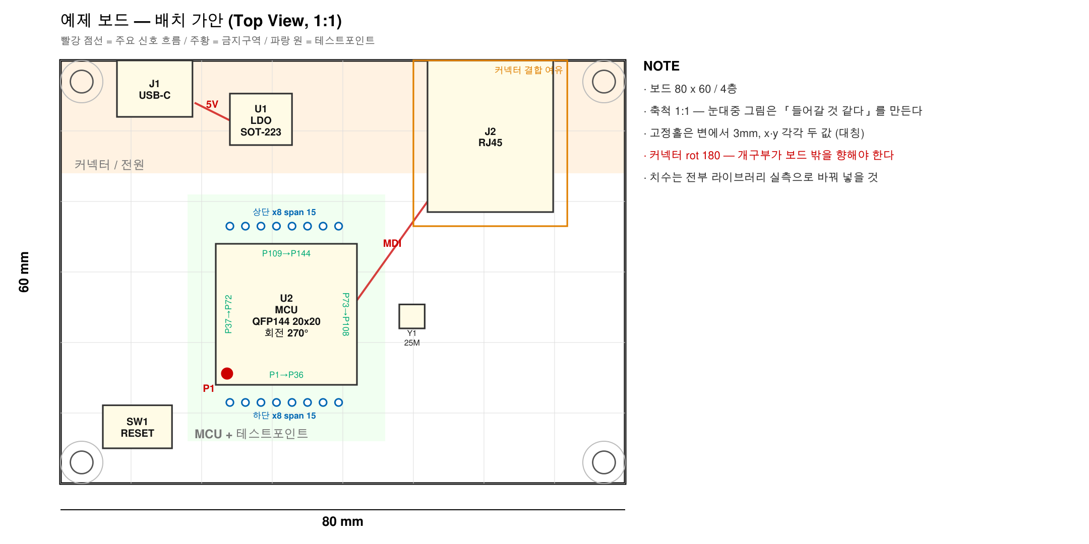
Placement actually proceeds like this:
1. Extract the connection matrix from the schematic   who connects to whom
2. Measure part dimensions from the library           never draw from nominal values
3. Derive board size by accumulating each axis        computed, not "about 100x100"
4. Decide main IC rotation from pin-to-side mapping   four options, with scores
5. Show a 1:1 plan drawing (SVG/PNG)                  <- 2-4 rounds here is normal
6. On approval, inject coordinates into the PcbDoc
7. Run overlap and out-of-board checks
Connectors, sockets and main ICs are placed with a stated reason. Resistors and capacitors are only gathered near their owning IC without overlapping — you place them finally. Where they belong is decided by routing intent, and encoding that as a rule costs more than it saves.
Two things it asks of you
- Save in Altium before any file-parsing step. The scripts read the file on disk. If Altium holds unsaved edits, you get answers about an old version
- Nothing is injected until you approve. Redrawing the plan is cheap and editing the PcbDoc is not. 2-4 rounds on the drawing is normal
What is actually in here
Each skill is SKILL.md (the procedure) + references/ (trap detail) +
scripts/ (runnable tools).
The 16 scripts
All of them run without Altium, because they parse the files with
altium_monkey. Claude calls them for you, but you can run them yourself —
they all take --help.
altium-library/scripts/
| Script | What it does |
|---|---|
survey_library.py |
Run this before authoring anything. Surveys what the library already holds. Having the symbol but not the footprint is common; author it blindly and you get a duplicate that nobody can later tell apart. Also searches by manufacturer abbreviation and pin count |
measure_drawing.py |
Measures hole coordinates and outlines from a vendor 2D drawing PDF as vectors. Drawing glyphs are vector outlines, so text extraction fails and eyeballing rendered pixels is wrong. It back-solves the pt/mm scale from a pitch you already know |
fit_symbol_body.py |
Computes the minimum symbol body size by exhaustive overlap test. Top and bottom pin names come in rotated 90°, so a small body makes names collide — and neither coordinate arithmetic nor an SVG render catches it |
audit_free_copper.py |
Finds free primitives on copper layers in a footprint. Regions, arcs and tracks carry no net, so a trace cannot enter a pad buried under them — and the symptom reads as a direction problem ("routing out of the pad works, into it does not"). Reports whether a pad is actually covered |
diff_symbol.py |
Compares a reference symbol against yours in three layers — parsed properties, record order (z-order), raw bytes. Comparing properties alone reported "identical" while the Altium canvas looked nothing alike |
altium-schematic-review/scripts/
| Script | What it does |
|---|---|
check_context.py |
Precondition check. Stops wasted work before review starts. The most common accident is reading the on-disk file while Altium holds unsaved edits, then concluding things like "there is no power section" |
net_erc.py |
Builds nets and runs four ERC-like checks. Counting only pins sitting on wires loses more than half the nets — this handles pin-to-pin, pin-to-power-port, and hidden pins |
audit_footprints.py |
Extracts footprint links from the schematic and reconciles them against real libraries. Catches "component with no footprint" before you move to PCB |
altium-pcb-placement/scripts/
| Script | What it does |
|---|---|
measure_from_lib.py |
Measures footprints from the schematic plus library folders, with no PcbDoc. You do not have to run Update PCB first |
connectivity_matrix.py |
Component-pair connection matrix plus per-pin partners for a reference part. Placement rationale is "who connects to whom, over how many nets". High-fanout power rails carry no information, so they are excluded |
pin_side_map.py |
Maps pin number to package side and scores all four rotations. For QFN/QFP the pin number determines the side, so this is computed, not a matter of taste |
connector_facing.py |
Determines which way a connector opening faces. The cable side has no pads, only housing — so it measures the pad bbox and the silkscreen bbox separately, and the side where silk protrudes further is the opening. No datasheet needed |
plan_svg.py |
Placement plan JSON to 1:1 scale SVG/PNG. A not-to-scale sketch produces "looks like it fits", and that is always wrong |
plan_to_placements.py |
Plan JSON to place_components input (mils). The plan is mm, lower-left origin, bbox; Altium is mils and component origin. These are not the same thing |
overlap_check.py |
Post-placement collision check. Layer-aware — opposite-side parts sharing XY is normal (that is where decoupling goes). Through-holes are the exception since they pierce the board, and they are compared one hole at a time (merging them makes a socket with four corner mounting holes flag everything beneath it). Pads-outside and silk-outside are reported separately |
apply_outline.py |
Inserts the board outline (rounded corners) and symmetric mounting holes. Writes a .bak first when editing in place |
Example — deciding connector rotation. python below is the venv python.exe
from install step 2, called by full path.
The script prints its column headers in Korean.
> python connector_facing.py board.SchDoc --libs C:\libs

des  개구부 돌출 mm     상변  하변  좌변  우변   풋프린트
J1   -Y       9.06      180    0   270    90   RJ45_J1B1211CCD
J2   -Y       2.21      180    0   270    90   USB-C_16P

숫자 = 그 변에 놓을 때 줘야 할 rotation (반시계 도).
des opening protrude mm top bottom left right footprint
Read it as: to put J1 on the top edge, rotate it 180°. No datasheet lookup required.
Reference documents (references/)
Most of what was expensive to learn lives here — roughly 1,400 lines of "this is how it breaks, and this is how you notice".
| File | What it saves you from |
|---|---|
altium-library/references/altium-monkey-api.md |
Unit convention (mils in, 10-mil out), pin names hidden by z-order, parameters landing at the wrong coordinates |
altium-library/references/tool-traps.md |
Where altium-mcp / eda-agent misbehave, and what the wrong answer looks like |
altium-library/references/drawing-measurement.md |
Vendor drawing glyphs are vector outlines. Eyeballing rendered pixels was wrong three times out of three |
altium-schematic-review/references/pin-verdict.md |
Deciding whether a floating pin is a real defect |
altium-schematic-review/references/altium-script-traps.md |
run_altium_script stalling in the debugger and blocking every MCP tool |
altium-schematic-review/references/net-build-notes.md |
Why a geometric netlist disagrees with the Altium compiler |
altium-pcb-placement/references/rotation-decision.md |
Deriving IC rotation from pin-to-side mapping; connector opening direction |
altium-pcb-placement/references/board-sizing.md |
Board size derivation, mounting hole symmetry, corner rounding |
altium-pcb-placement/references/injection.md |
Component origin is not bbox center; the authoring builder swallowing direct edits |
altium-pcb-placement/references/plan-schema.md |
The plan.json format. A working example is in examples/ |
What works without Altium
| Needs Altium | Files only | |
|---|---|---|
| Library authoring / verification | Visual confirmation | Generation, comparison, measurement |
| Schematic review | Compiled-net cross-check (optional) | Net build, ERC-like checks, footprint reconciliation |
| PCB placement | Coordinate injection, screenshots | Dimension measurement, rotation math, plan drawing, overlap check |
A placement plan for an outside PCB design house can be produced with no Altium at all — the schematic and libraries (or datasheets) are enough.
When it does not work
| Symptom | Cause and fix |
|---|---|
altium_monkey import error |
You ran the python on PATH. Call the venv's python.exe by full path |
pip install altium-monkey fails |
You are on Python 3.13+. The package requires <3.13. Rebuild the venv with py -3.12 -m venv |
| The skill never triggers | (1) Check the junction is under ~/.claude/skills/. (2) Open a new Claude Code session — a skill linked mid-session does not appear in that session |
| Review disagrees with what is on screen | Altium has unsaved edits. The scripts read the file on disk. Ctrl+S, then rerun |
| The outline and holes you added disappear | Altium had that PcbDoc open. Altium overwrites the file when it saves. Close it, or have the user save first, run, then reload |
| Every MCP tool stops responding | run_altium_script hit a runtime error and is stalled in the Altium debugger. Press Ctrl+F3 in the Altium window. Because the scripting slot is global, this blocks the other MCP tools too |
| A connector is reversed but every check passes | A bbox does not change under 180° rotation. Overlap and outline checks cannot see it. Use connector_facing.py to check the opening direction separately |
| A part sits a few mm off the plan | Component origin is not bbox center. A footprint origin may be pad 1, the body center, or somewhere else. plan_to_placements.py corrects for it — do not hand-enter coordinates |
Contributing
Issues and PRs welcome. Two rules keep this useful.
- Write rules, backed by measured numbers. Do not narrate what went wrong.
QFN32 body 4.00 -> actual footprint 7.05x7.00is the information - No specific chip or board names, and no values from one design. These are general-purpose skills; the verdict comes from the datasheet each time
No comments yet
Be the first to share your take.